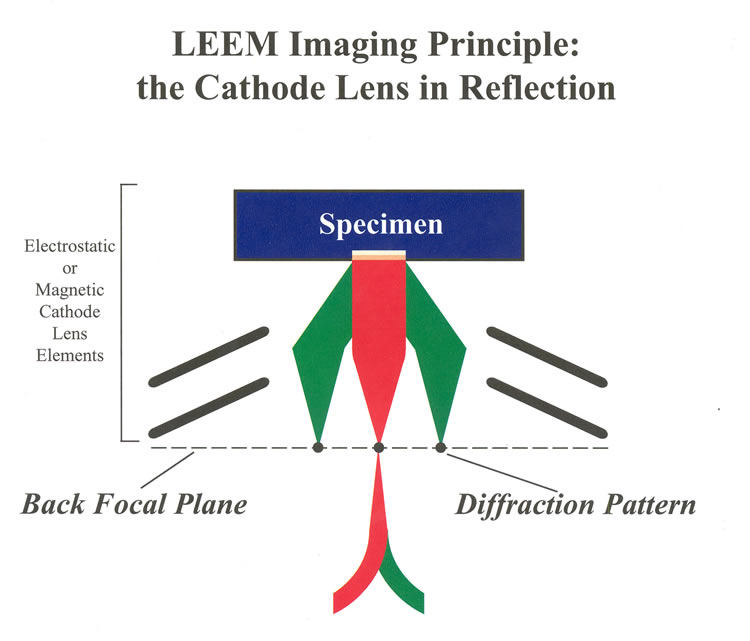
LEEM is fundamentally
an emission microscopy. In conventional emission microscopy,
electrons are emitted by some external stimulus, e.g.,
photo, thermal, or secondary emission. In LEEM, electron
emission is stimulated by a coherent (collimated,
monoenergetic) electron beam at or near normal incidence
angle. First of all, an electron beam is generated
by the cathode in the electron gun and accelerated
up to the microscope potential, typically 20 keV.
The illumination optics, consisting of a sequence
of lenses and apertures, is then used to form a collimated
electron beam suitable for illumination of the sample.
Before reaching the sample, the beam must pass through
a magnetic sector field that deflects the beam typically
by 60 degrees. The magnetic sector field serves the
important purpose of separating the beam that is reflected
from the surface (green
in Fig.1)
from the incident beam (red
in Fig.1). The incident electron beam is focused by
the illumination optics to a point in the back focal
plane of the objective lens (Fig.1),
which is the heart of the LEEM. The incident and reflected
beam that has undergone no momentum transfer parallel
to the surface are overlapping in the objective region.
The objective lens acts on both the incident and reflected
electron beams and serves a dual purpose in both instances.
In the objective, the incident beam is simultaneously
focused to a parallel beam and decelerated to the
desired incident energy that is given by the bias
between the sample and the electron gun cathode. For
crystalline samples, the backscattered beam will be
confined to several specific angles - the Bragg angles
- by diffraction. These electrons are then reaccelerated
by the objective up to the microscope potential and
focused to points in the back focal plane. This forms
a diffraction pattern in the back focal plane. The
reflected beam is then deflected by the sector field
into the imaging column, which consists of a number
of lenses. An image is formed by selecting one of
the diffracted beams with a contrast aperture in the
imaging column and magnification of this beam onto
the microchannel plate image intensifier and phosphor
screen. So-called bright field imaging is performed
when the (00) or specular beam is used to form an
image. The electrons in this beam have undergone no
momentum transfer parallel to the surface. Tilted
bright-field imaging also employs the (00) beam, but
with a slight tilt of the illumination from normal
incidence. Finally, dark-field imaging utilizes a
non-specular fractional or integer order diffraction
beam for imaging. Alternatively, the entire diffraction
pattern may be viewed. This capability of imaging
and diffraction allows a direct comparison of real
and reciprocal space features.
Real-time Imaging [Top]
Three important aspects
of LEEM permit real-time imaging at video rates. First,
LEEM is a non-scanning technique. That is, every point
in the region of the surface that is being imaged
is illuminated simultaneously and every point in the
image is detected in parallel. Secondly, the reflected
intensity for very low incident energies can be very
high, reaching as much as 50% of the incident intensity
for incident energies below 10 eV. For comparison,
reflected intensities are typically one to three orders
of magnitude smaller at incident energies, 50 - 300
eV, that are used in conventional low energy diffraction.
Finally, the reflected intensity is confined to the
diffraction angles for crystalline samples. The combination
of parallel illumination/detection and high reflected
intensity confined within small angles of specific
directions by diffraction is favorable for fast imaging
acquisition. Although the reflected intensity at higher
energies or for non-crystalline sample may not allow
imaging at video rates, images may still be obtained
at slower rates by signal integration, provided that
ccd cameras with suitably low noise are used.
Spatial Resolution [Top]
The spatial resolution
of LEEM is determined by the aberrations of the objective
lens and by diffraction at the contrast aperture.
At very low energy, LEEM is diffraction limited. The
resolution of LEEM is primarily limited otherwise
by chromatic aberrations. Calculations for an ideal
homogeneous acceleration field [2]
indicate that the ultimate resolution of LEEM would
be on the order of 2 nm. Real objective lenses are
only approximations of the ideal homogeneous acceleration
field. The LEEM at HKUST employs a magnetic objective
lens and has a spatial resolution of about 5-7 nm
depending upon the incident energy. Phase contrast
mechanisms, which are described below, give LEEM atomic
resolution perpendicular to the surface.
Depth sensitivity [Top]
According to the "universal
curve" for electron mean free paths, the minimum
penetration electron depth of just a few Å occurs
at an incident energy of about 50 eV. The mean free
path increases at lower energies appropriate for LEEM
imaging. At very low energies, i.e., below 10 eV,
the penetration depth may even approach 100 Å.
This indicates that LEEM is generally sensitive to
the topmost several atomic layers, but that deeper
layers may also be probed by using very low incident
energies. This fact is attested to by measurements
of the quantum size effect in the reflection of low
energy electrons [3,4],
which demonstrate that interfaces that are buried
at least 9 atomic layers below the surface can be
detected.
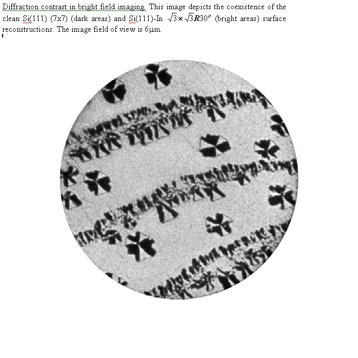
Contrast [Top]
Contrast mechanisms
in LEEM conventionally falls into two categories:
diffraction and phase constrast. Diffraction contrast
occurs due to local variations of the structure factor.
Diffraction contrast arises, for example, in bright-field
imaging at normal incidence/exit because of geometric
structure differences between different phases (Fig.2).
Diffraction contrast is also important in tilted bright-field
imaging. A well-known example is the Si(100) (1x2)
surface. The surface structure consists of dimer rows
which run parallel to either the surface (100) or
(010) direction, and is called accordingly (1x2) or
(2x1) to reflect the rotational relationship. Because
of the bulk stacking, the dimer row direction rotates
by 90 degrees on adjacent terraces, which leads to
a topographical domain structure. Due to the strong
dependence of the reflected intensity upon the incident
angle on this highly anisotropic surface, a strong
difference of the reflected intensity is realized
between the (1x2) and (2x1) domains when the incident
beam is tilted slightly in the (100) or (010) directions
(Figs. 3,
4). Such a tilt may be
parallel to the dimer rows in the (1x2) domains and
perpendicular to the rows in the (2x1) domains, or
visa-versa.
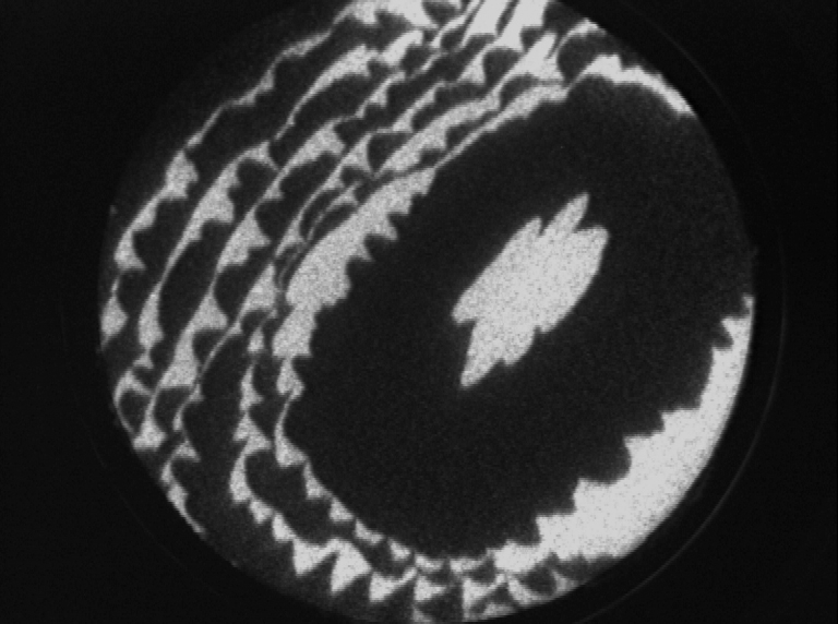
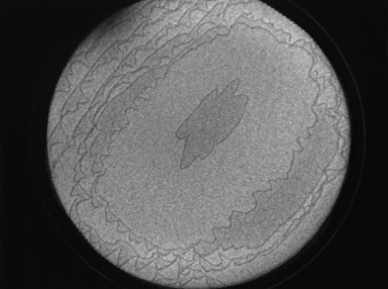
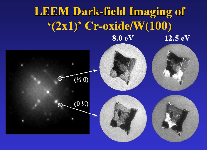
Diffraction contrast
is also important in dark-field imaging. Dark-field
imaging is especially useful for identifying the spatial
distributions of coexisting phases or when the small
tilt angles used in titled bright field imaging are
not sufficient to obtain contrast between rotational
variants of low symmetry structures. An example from
our work on Cr oxidation on the W(100) surface [5]
is shown in Fig.5.
In this example, dark-field images of three-dimensional
Cr-oxide crystals are formed using the (½ 0)
and (0 ½) diffraction spots. The areas in the
crystal "light up" when they contribute
to the diffraction spot used for imaging. These images
clearly show the complex, complementary domain microstructure
of the Cr-oxide crystals.
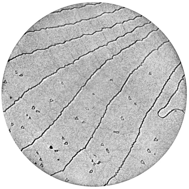
One important class
of LEEM contrasts are those having their origin in
the phase of the imaging electron waves. Two important
examples of LEEM phase contrast are atomic step contrast
[3,6] and quantum
size contrast [3,4].
Both of these phase contrasts provide atomic resolution
information perpendicular to the surface. LEEM step
contrast arises from the interference of the electron
waves which are reflected from terraces on opposite
sides of a step. The interference is a consequence
of the phase shift that stems from the path length
difference of the two waves. Since the wavelength
of the electrons in the very low energy regime appropriate
for LEEM is on the order of the step height, a wide
range of phase shifts, and consequently interference
conditions, can be sampled by making small changes
of the imaging electron energy. A wave-optical model
for LEEM step contrast has been developed [3,6].
Step contrast is calculated as the interference of
the Fresnel diffracted waves from the terrace edges
which meet at a step. This model allows for the routine
identification of the step sense, i.e., the up and
down-sides of a step, by simple visual inspection.
Sample images that show step contrast are shown in
Fig.6.
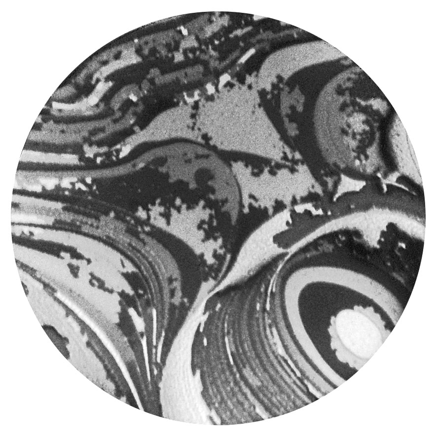
Quantum size contrast
is a vivid manifestation of the quantum size effect
(QSE) in electron reflectivity. This QSE is understood
classically to be an interference phenomena between
the electron waves which are reflected from the surface
of a thin film and from its interface with the substrate.
A simple quantum mechanical Kronig-Penney model has
been developed which accurately predicts the modulation
of the reflected intensity as a function of film thickness
and incident electron energy that is caused by the
QSE [3,4]. A
sample image that shows quantum size contrast is shown
in Fig.7.
Operation conditions of
LEEM [Top]
LEEM is an ultra-high
vacuum instrument, with typical base pressure of 1x10⁻¹⁰
torr and operational pressure under experimental conditions
of up to 10-6 torr, or possibly higher.
The pressure limitation during experimental operation
is imposed by high voltage isolation between the sample
and objective lens. LEEM can be operated continuously
during deposition of metals or semiconductors or during
gas exposure, including reactive gas. Imaging may
also be performed over a wide range of temperature.
The minimum temperature of operation so far that was
achieved at HKUST was 50K, which was limited by the
sample cooling apparatus. This is also a world record.
LEEM also functions well at higher temperatures. Our
experience shows that imaging is possible as high
as 1500 K and possibly higher, depending upon the
sample characteristics. At HKUST, we have also developed
a sample holder with which it is possible to apply
up to 100 G magnetic field at the sample position.
Deflection of the imaging electron beam by magnetic
fields parallel to the surface causes a sever limitation
in working with applied magnetic fields in LEEM. Therefore,
only magnetic field that is perpendicular to the sample
can be applied conveniently in-situ during imaging.